 | Services and Modeling for Embedded Software Development |
|---|
| Services and Modeling for Embedded Software Development |
|---|

Application Note 14. Issue 1.0
November 2015
Copyright © 2015 Embecosm Limited
 | The document entitled " AAP: An Altruistic Processor " by of Embecosm is licensed under a Creative Commons Attribution 2.0 UK: England & Wales License. See the Legal Notice for details. |
Table of Contents
NOP commandsIt was a bright cold day in August, and the clocks were striking 50 million times a second. Dan's implementation of an AAP processor is complete, and he's ready to share it with the world.
I am a student, with no previous knowledge of making a processor. Therefore this is my first attempt, and is by no means a definitive guide to creating a processor. Its purpose is to allow a novice to grasp the basics via an easy to understand processor.
We will take our design from Embecosm®'s previous application note, AAP: An Altruistic Processor. Our hardware description language of choice will be Verilog, which if you have not come across will look a lot like C. For this Application Note you will not need to already know Verilog, but it would be advisable to have a quick read and play with my last application note: ChipHack For Teens.
This guide is primarily focused at Linux users, however the ideas are the same regardless of operating system.
![[Note]](./images/note.png) | Note |
|---|---|
|
You can always trial Linux on your machine, most distributions are free. I would recommend something like ElementaryOS[1] for a beginner. |
It is also advised to have IVerilog and GTKwave installed for simulation on your computer.
As this Application Note is written to be used with a DE0 Nano, to put the processor onto the FPGA we will be using Quartus® software.
We all know we have a CPU in our computers, which Simon Lane correctly confirmed stands for Central Processing Unit not Computer Processing Unit[2]. Processors are the components in computers which are responsible for the computation and flow control, the adding and subtracting and moving from here to there.
That's nice. A GHz is a measurement of how fast the clock of the processor is. For example if you were to buy a Raspberry Pi 2, that has a clock speed of 250MHz, you would get a processor that has a clock that can switch on and off 250,000,000 times a second! Or if you were to steal my phone, with a clock speed of 2.5GHz you would have a a clock that can switch on and of 2,500,000,000 times a second!
| Note |
|---|---|
|
Please don't steal my phone. |
At the heart of it a processor is just a bunch of wires that are either on or off (unless you are working with a quantum computer, in which case this is probably not the guide you are looking for[3]). There are numerous different stages in a processor.
Fetch will see the program counter (the address of the current instruction) and go look up this address in our instruction memory, where all tasks are being kept.
From our fetch stage we get a random looking number, this is where we give it a purpose! This stage changes a long string of binary into a more meaningful representation that Execute will use.
A common mistake, Harvard actually refers to Harvard architecture not John the politician. A significant difference about AAP and normal (von Neumann) processors is that it uses the Harvard Architecture model where data and instructions are kept in separate memories instead of one. This is useful for security as one common hack is to load data whilst tricking a processor into thinking you are loading instructions, and then executing the data.
Before we start designing our processor we must know what it needs to be capable of, so we can choose useful blocks for its implementation.
As we know our processor is a Harvard architecture, therefore we will need to program 3 separate memories, which we can read and write to (and from).
We need an instruction memory, so we can store what we want to happen, a list of things for the processor to execute.
Is where we keep information long term, where we can store it. This will be the smallest of the memories, with a width of only a byte (8 bits).
An AAP processor is capable of executing instructions that are both 16 and 32 bits in size. Therefore our processor must be able to determine which it has received and act accordingly.
The AAP architecture specification lists over 50 different operations which we will need to implement. But what do they all mean?
It may sound simple but in the future it will assist with the debugging of the board and therefore becomes not as simple.
An add takes the value from two registers, sums them and places in another designated register.
I hear you wonder What is the difference between unsigned and signed Dan?. Well an unsigned value is just whatever value it is, but cannot be less than 0. However a signed number has a special bit at the top which tells us if it is negative, using a system called two's compliment. Don't worry, we wont have to do any fancy code for that.
A subtract takes the value from two registers, takes away the second from the first and places in the designated register.
This will take two registers and complete an AND when comparing the two in binary. for example:
10101001
00101111
________ AND
00101001
This can only be a 32 bit instruction, and bitwise ANDs the number in the register with a given value.
This is similar to AND, however with an OR, if the same bit in either value is 1 the output is 1.
10101001
00101111
________ OR
10101111
This can only be a 32 bit instruction, and it bitwise ORs the number in the register with a given value.
For this instruction, the output is 1 if and only if one of the operand is 1, otherwise it is 0.
10101001
00101111
________ XOR
10000110
This can only be a 32 bit instruction, and it bitwise XORs the number in the register with a given value.
This instruction moves all the bits along by the amount in the register given, effectively doubling the number.
This instruction will move all the bits along by the amount in the register given, but to the right, effectively halving the number.
This is used in conjunction with two's compliment signed numbers. It is similar to a logical shift right however the new bit(s) is the same as the sign bit. It's shifted by the amount in the register given
This instruction puts the value of one register into this other register.
This instruction adds the register given plus the number given, placing the result into the destination register.
This instruction takes the number given away from the value in the register given and place in the register designated.
This instruction is exactly the same as the normal Arithmetic shift, but instead it shifts by an amount given in the command.
This instruction shifts all the bits along to left by this amount.
This instruction shifts all the bits right by this amount to the right.
Look up the byte destination you are given and load only 8 bits into your 16 bit register.
Look up a byte and load it into your register and then load up the next byte as the second part of your register to load a full 16 bits.
Look up in Data memory the value you are given in the register and store it into the destination register you are given, but increment the memory reference once complete.
Look up in Data memory the value you are given in the register and store it into the destination register you are given, but increment the memory reference once complete.
Look up in Data memory the value you are given in the register and store it into the destination register you are given, decrementing the memory reference before the load.
Look up in Data memory the value you are given in the register and store it into the destination register you are given, decrementing the memory reference before the load.
Put the value of the register you are given into the place in data memory from the register with the value of destination.
Put the value of the register you are given into the place in data memory from the register with the value of destination.
Put the value of the register you are given into the place in data memory from the register with the value of destination, but increment the memory reference once complete.
Put the value of the register you are given into the place in data memory from the register with the value of destination, but increment the memory reference once complete.
Put the value of the register you are given into the place in data memory from the register with the value of destination, decrementing the memory reference before the store.
Put the value of the register you are given into the place in data memory from the register with the value of destination, decrementing the memory reference before the store.
Move the program counter along by this many, to skip out the instructions between.
Move the program counter along by this many, to skip out the instructions between. But save a record of the program counter into a register to enable a return to this point later.
Only change the program counter if these two registers are different.
Only change the program counter if the first register is smaller than the second.
Only jump the program counter if the first register is larger than the second.
Only change the program counter if the first register is smaller than the second.
Only jump the program counter if the first register is larger than the second.
Make program counter equal to the value in the given register. But save a record of the program counter into a second register to allow us to return to this point.
Make program counter equal to the value in the given register if the specified two other registers are equal.
Make program counter equal to the value in the given register if the specified two other registers are different.
Make program counter equal to the value in the given register if the first register is smaller than the second.
Make program counter equal to the value in the given register if the first register is larger than the second.
Make program counter equal to the value in the given register if the first register is smaller than the second.
Now we understand what our processor needs to do, we shall draw our design, so that we can understand how all the parts work together.
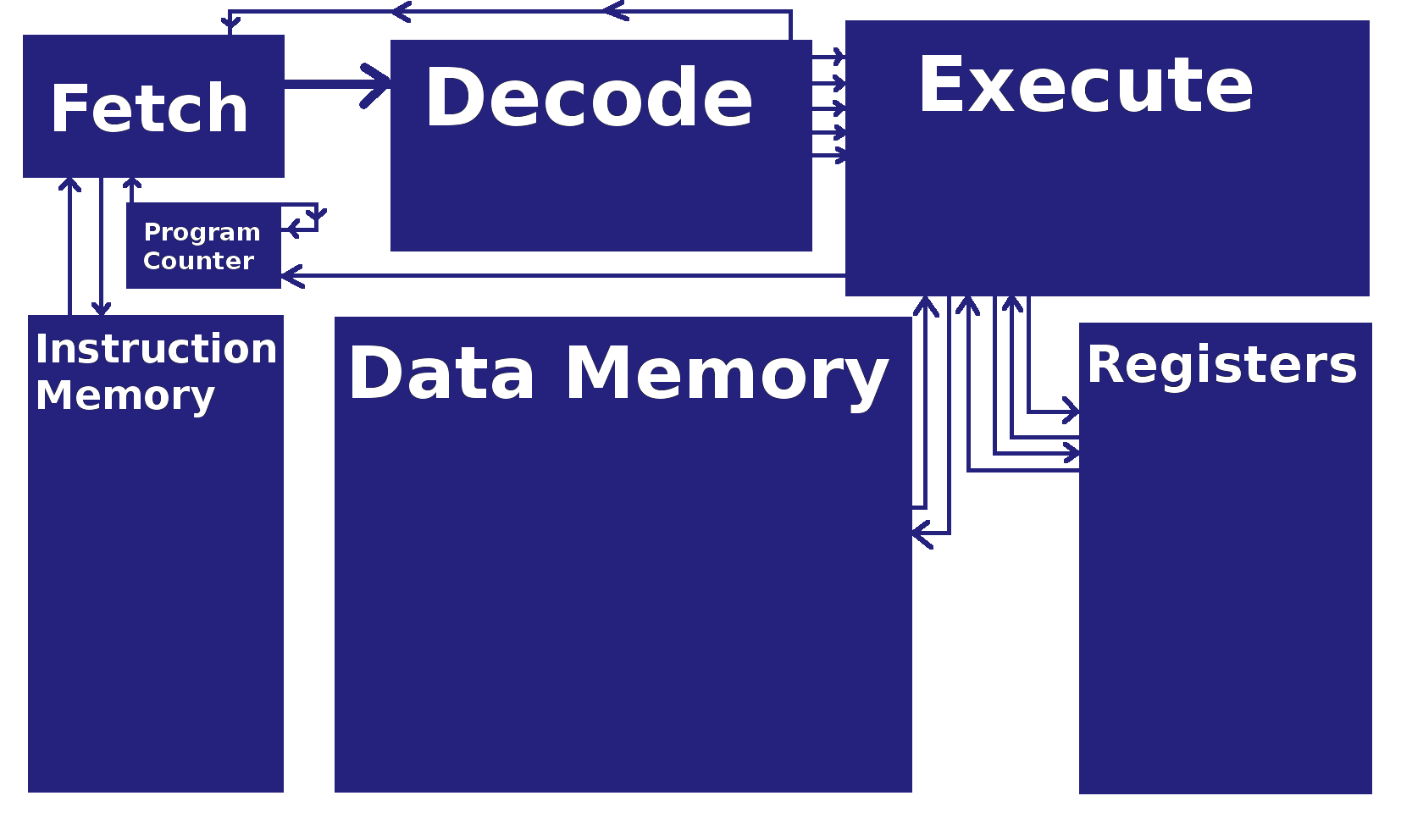 |
Our fetch will get a signal from the program counter, read an instruction from instruction memory and output it to the decoder.
| Note |
|---|---|
|
Our program counter will also be inside the fetch module, though it is common to show it as part of the registers. |
Our decoder will get a long binary number and will split it up into recognizable chunks and send those of to execute. Also it might occasionally send a flush signal to fetch if it detects a 32 bit command, as a 32 bit command will be made up of two separate 16 bit commands, but we do not want the second 16 bit command to run on its own as it would not work.
Execute will receive the set of inputs from decode, and determine what it is doing by an operation number input. It might then need to write to the data memory or the registers, and it might need to change the program counter for the jump operations, depending on the instruction that was decoded.
The first thing we will make is a decoder, as it can work on its own and we can then try debugging it in GTKwave.
An important concept in our processor is that you can have 16 and 32 bit
instructions. But how do you know how much data needs to be fetched?
Instead of some complex mess we fetch a 16 bit instruction that becomes
the bottom half of fetchoutput. On the next clock
cycle, this becomes the upper half of fetchoutput and
a new bottom half appears. We only read the top half during decode
unless it indicates to us that the instruction is really 32 bits long,
in which case we then use the entire 32 bit word.
So we can actually get stuff done.
We need to break down our 16 bit number into something that will be useful for the execute stage.
This is where we look at the Application Note for AAP. For example, we may get an instruction like this:
0000001100001010
This word is supposed to tell us to add register 1 to register 2 and put the result in register 3. Fortunately all similar commands have a similar encoding. For example an add instruction can be shown generically as:
0000001dddaaabbb
The first digit on all instructions tells us whether it is 16 or 32
bit. A 0 indicates 16. The next 6 bits tells us the operation
number. The next 3 bits will almost always tell us the destination
register (d). a stands for first
source and b for second source.
With this knowledge we can make our decoder always make destination
equal to bit 6, 7 and 8. We can also always assign
a and b equal to where they are
in this 16 bit command. It doesn't matter if we don't use this in
execute. If we look at the list of instruction we can see other
formats. lots of the instructions have three is
instead of bs, so we will need to decode these into
another value.
In short, we need to group up the different parts of the instructions so we can refer to those by name in our execution module.
We start our decoder module by declaring its inputs and outputs:
module Decoder ( fetchoutput,
                 destination,
                 operationnumber,
                 source_1,
                 source_2,
                 unsigned_1,
                 unsigned_2,
                 unsigned_3,
                 unsigned_4,
                 unsigned_5,
                 signed_1,
                 signed_2,
                 signed_3,
                 super_duper_a,
                 super_duper_b
              );
"What are all those outputs?" I hear you cry. Well these are what we
are going to be splitting fetchoutput into. Those
are all the groups in all the combinations of instructions.
We need to make sure we have all the right inputs and outputs. We need to declare all the Verilog registers.
// Registers //
reg         operation;
reg [05:00] destination;
reg [05:00] source_1;
reg [05:00] source_2;
reg [05:00] unsigned_1;
reg [15:00] unsigned_2;
reg [08:00] unsigned_3;
reg [09:00]   unsigned_4;
reg [08:00] unsigned_5;
reg [05:00] operationnumber;
reg [21:00] signed_1;
reg [15:00] signed_2;
reg [09:00] signed_3;

reg super_duper_a; // used for 32 bit instructions that cannot
reg super_duper_b; // be different using operation number alone


// Wire Declarations //
wire [31:00]    fetchoutput;
wire            bit_check;
To check whether an instruction is 32 or 16 bit we define the wire
bit_check. If an instruction is 32 bits long then
the first digit is a 1 else it will be 0. We will assign
bit_check to equal the first digit:
assign bit_check = fetchoutput[31];
If the instruction is 32 bit we will decode it differently.
We always want to decode when we detect a new
fetchoutput.
always @(fetchoutput) begin
First we check if it is 16 bit, is so we will decode accordingly:
if (bit_check == 0) begin
   operationnumber  = fetchoutput [30:25];
   destination      = fetchoutput [24:22];
   source_1         = fetchoutput [21:19];
   source_2         = fetchoutput [18:16];
   unsigned_1       = fetchoutput [18:16];
   unsigned_2       = fetchoutput [21:16];
   unsigned_3       = fetchoutput [24:16];
   signed_1         = fetchoutput [24:16];
   signed_2         = fetchoutput [24:16];
   signed_3         = fetchoutput [24:16];
   super_duper_a    = 0;
   super_duper_b    = 0;
end
We know where in fetchoutput each group is thanks
to the AAP documentation. However if an
implementation is being made for a different architecture, these are
probably all different.
As you remember fetchoutput actually contains 2
instructions so when it is only 16 bits we only refer to the top
one. super_duper is not needed for 16 bit
instructions.
Otherwise, if we detect that the instruction is 32 bits long, we decode it as follows:
else if (bit_check == 1) begin

   destination[02:00] = fetchoutput [24:22];
   destination[05:03] = fetchoutput [08:06];
   source_1[02:00]    = fetchoutput [21:19];
   source_1[05:03]    = fetchoutput [05:03];
   source_2[02:00]    = fetchoutput [18:16];
   source_2[05:03]    = fetchoutput [02:00];
   unsigned_1[02:00]  = fetchoutput [18:16];
   unsigned_1[05:03]  = fetchoutput [02:00];
   unsigned_2[05:00]  = fetchoutput [21:16];
   unsigned_2[09:06]  = fetchoutput [12:09];
   unsigned_2[15:10]  = fetchoutput [05:00];
   unsigned_4[02:00]  = fetchoutput [18:16];
   unsigned_4[06:03]  = fetchoutput [12:09];
   unsigned_4[09:07]  = fetchoutput [02:00];
   unsigned_5[02:00]  = fetchoutput [18:16];
   unsigned_5[05:03]  = fetchoutput [12:08];
   unsigned_5[08:06]  = fetchoutput [02:00];
   signed_1[08:00]    = fetchoutput [24:16];
   signed_1[21:09]    = fetchoutput [12:00];
   signed_2[02:00]    = fetchoutput [24:22];
   signed_2[05:03]    = fetchoutput [18:16];
   signed_2[12:06]    = fetchoutput [12:06];
   signed_2[15:13]    = fetchoutput [02:00];
   signed_3[02:00]    = fetchoutput [24:22];
   signed_3[09:03]    = fetchoutput [12:06];
   operationnumber    = fetchoutput [30:25];

   if (fetchoutput[15:09] !== 0) begin    // for 32 bit commands that have
                                          // the same opcode but extra
                                          // criteria
      super_duper_a = 1;
   end

   if (fetchoutput[9] !== 0) begin        // for the bitwise commands
                                          //that need to be different
      super_duper_b = 1;
   end
   else begin
      super_duper_a = 0;
      super_duper_b = 0;
   end
end
super_duper is used for 32 bit instructions such as
"Bitwise AND immediate" where the only way to tell the difference
between the immediate and the normal is whether
super_duperis set to 1.
In 32 bit instructions the operand size is double the size for each group compared to the 16 bit variants. We take the bits assigned to each group in the bottom half of the instruction and place them in front of the other to produce the correct number.
So you've made a decode module. Well you think you have, but you have no idea if it works or not yet.
We will be using Icarus Verilog and GTKwave to analyze our decoder.
You can quickly check that your Decode module has no syntax errors using Icarus:
$ iverilog <file.v>
A test bench will output a file that GTKwave can open, so we can view the values of every wire and register, over a period of time.
We shall be making our test bench in another .v file in the same
directory. Before we declare our module, we have to state that this
file will also be using our decode file. This is done by importing
it using a `include command:
`include "<filename.v>"
The test bench module will not need any inputs and will have no outputs. However we need to declare lots of wires inside of the module, so they can be connected to the modules we want to test inside.
module testbench;

   wire         operation;
   wire [05:00] destination;
   wire [05:00] source_1;
   wire [05:00] source_2;
   wire [05:00] unsigned_1;
   wire [15:00] unsigned_2;
   wire [08:00] unsigned_3;
   wire [09:00] unsigned_4;
   wire [08:00] unsigned_5;
   wire [05:00] operationnumber;
   wire [21:00] signed_1;
   wire [15:00] signed_2;
   wire [09:00] signed_3;

   wire super_duper_a; // used for 32 bit instructions that cannot
   wire super_duper_b; // be different using operation number alone

   reg clock;
   reg reset;

   reg [31:00]    fetchoutput;
   wire            bit_check;
We then create a copy of the module(s) we want to debug in the test bench and connect their inputs and outputs with the wires and registers we have created.
    decoder decoder_test (
                           fetchoutput[31:00],
                           destination[05:00],
                           operationnumber[05:00],
                           source_1[05:00],
                           source_2[05:00],
                           unsigned_1[05:00],
                           unsigned_2[15:00],
                           unsigned_3[08:00],
                           unsigned_4[09:00],
                           unsigned_5[08:00],
                           signed_1[21:00],
                           signed_2[15:00],
                           signed_3[09:00],
                           super_duper_a,
                           super_duper_b
                         );
Next we write the code to create a vcd file to
log changes that occur in our decoder. We can use this later with
GTKwave to investigate
these changes.
   initial begin
      $dumpfile ("<destinationfilename.vcd>");         // Where to put
      $dumpvars (0, <testbench_version_of_module>);    // What to put

      #20                            // Wait 20
         fetchoutput = 2147483647;   // after 20 set fetchoutput to ...
      #20
         fetchoutput = 1;
      #20

      $finish
The syntax to tell the test bench to dump all the files in a module is:
$dumpvars (0, <module>)
The hash followed by a number is a wait, so in total we will have 60
seconds worth of decoding analyze. Make sure to change
fetchoutput after an amount of time otherwise the
waves will be flat. The test bench stops once the
$finish is executed.
Now you can run this program through Icarus Verilog the same as any other file. In your terminal, in the correct directory, run:
$ iverilog testbench.v
$ ./a.out
Then open the VCD it created with GTKwave.
$ gtkwave <outputfile.vcd>
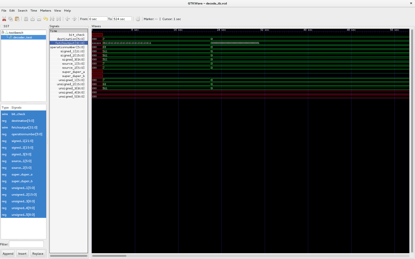 |
In GTKwave, you can
insert all the wires and registers from
decoder_test and (hopefully) view them change
after 20 seconds.
This chapter sounds too much like a romantic novel that has just won Waterstone™'s Best Book of the Year award.
Before we can make an execute module to do stuff with our working decoder, the execute will need somewhere that it can read and write data to and from.
As you recall, we have three memories that we will need to make: the instruction, data and the registers. These should all be rather easy to make as after we make one you can just copy it and change a few of the values and names
Although we will not be writing to this memory yet we will prepare it now for the future.
module TheInstructionMemory (   clock,
               reset,
               instruction_rd1,
               instruction_rd2,
               instruction_rd3,
               instruction_rd4,
               instruction_wr1,
               instruction_wr2,
               instruction_wr3,
               instruction_wr4,
               instruction_wr1_data,
               instruction_wr2_data,
               instruction_wr3_data,
               instruction_wr4_data,
               instruction_wr1_enable,
               instruction_wr2_enable,
               instruction_wr3_enable,
               instruction_wr4_enable,
               instruction_rd1_out,
               instruction_rd2_out,
               instruction_rd3_out,
               instruction_rd4_out
               );
   input clock;
   input reset;

   // This register has eight ports: four read, four Write

   // read inputs and outputs //

   input  [07:00] instruction_rd1;           // Which register to read from
   input  [07:00] instruction_rd2;           // 8 bits wide because we
   input  [07:00] instruction_rd3;           // have up to 128 data
   input  [07:00] instruction_rd4;

   output [15:00] instruction_rd1_out;       // What is in that register
   output [15:00] instruction_rd2_out;
   output [15:00] instruction_rd3_out;
   output [15:00] instruction_rd4_out;

   // write inputs and outputs //

   input  [07:00] instruction_wr1;           //Where to write, which register
   input  [07:00] instruction_wr2;
   input  [07:00] instruction_wr3;
   input  [07:00] instruction_wr4;

   input  [15:00] instruction_wr1_data;      //What to write
   input  [15:00] instruction_wr2_data;
   input  [15:00] instruction_wr3_data;
   input  [15:00] instruction_wr4_data;

   input          instruction_wr1_enable;    //Should it write
   input            instruction_wr2_enable;
   input          instruction_wr3_enable;
   input            instruction_wr4_enable;
We will be using the same clock throughout all our modules. We can change this clock to either be one we make when running through Icarus Verilog or to have it be bound to a clock generator on the FPGA.
Also for our instruction memory we will have 4 reads and 4 writes. However we will only be using one read for now.
We now need to actually make the memory block. We want ours to be quite small for now, and has to be only 16 bits long, as this is the size of the smallest instructions.
reg [15:00] instruction_memory [128:00];
To read a register you set instruction_rd the
location you want to read, the corresponding
instruction_rd_out output will then tell you what
is in that location.
   // Read logic //
   // This is combinatorial, it happens automatically

   assign instruction_rd1_out = instruction_memory[instruction_rd1];
   assign instruction_rd2_out = instruction_memory[instruction_rd2];
   assign instruction_rd3_out = instruction_memory[instruction_rd3];
   assign instruction_rd4_out = instruction_memory[instruction_rd4];
Previously everything has been combinatorial, it just happens. But for our write we want it to happen on the clock edge, so it is sequential.
We only want to write to the designated location if it has been enabled. We also want to have a reset condition in here so we can load a program in from a file.
   always @(posedge clock or posedge reset) begin
   // this is sequential, it will only happen on the clock or reset

      if (reset == 1) begin
         $readmemb("instructionmemory.list", instruction_memory);
      end

      else begin

         if (instruction_wr1_enable == 1) begin
            instruction_memory[instruction_wr1] = instruction_wr1_data;
         end

         if (instruction_wr2_enable == 1) begin
            instruction_memory[instruction_wr2] = instruction_wr2_data;
         end

         if (instruction_wr3_enable == 1) begin
            instruction_memory[instruction_wr3] = instruction_wr3_data;
         end

         if (instruction_wr4_enable == 1) begin
            instruction_memory[instruction_wr4] = instruction_wr4_data;
         end
      end
   end
On our reset we set all the value in instruction_memory to those in
instructionmemory.list. The list is a separate file
that we keep in the same directory. We change this file to be able to
add in instructions for our processor.
| Note |
|---|---|
|
Make sure to remember the |
The Register module looks very similar however
there are only five ports: 2 write, 3 read. The size is a lot smaller,
as the register bank is much smaller than the instruction memory.
reg [15:00] register [31:00];
| Note |
|---|---|
|
You can change any of these sizes, but make sure that you are able to access all of them. |
Similarly we also read an initial state from a file on reset.
   if (reset) begin    // Reset all Registers
      $readmemb("register.list", register);
The Data memory is the smallest (in terms of width). It is instead 8 bits wide and can be up to 65,535 items deep (as that's the biggest value you can give with the 16 bits), though we can give it any size we want up to this value.
reg [07:00] data_memory [127:00];
Make sure to declare all the inputs and outputs you need at the right size. This will be very similar to the instruction memory above.
We are resetting our memories by reading from a list file. To make these, open your text editor and create the appropriate amount of lines of binary in the format:
0000_0000_0000_0000
| Note |
|---|---|
|
Make sure to save into the same directory as the Verilog files. |
Remember for all the commands you want nothing to happen on you need
to use a NOP no operation which is different to
leaving sixteen zeros (For AAP at least).
Now we can add the memories to the test bench so they can be accessed by other modules.
You only need to define wires that are shared across modules in the test bench, so we do not need to make another data_memory register.
| Note |
|---|---|
|
Remember to add the |
Also, like the decoder_test, we need to make
memory_tests. We can simply copy over the start to
the modules including the bracketed inputs and outputs and add a copy
of the module name with _test appended to the end.
   TheInstructionMemory TheInstructionMemory_test
                           (
                             clock,
                             reset,
                             instruction_rd1,
                             instruction_rd2,
                             instruction_rd3,
                             instruction_rd4,
                             instruction_wr1,
                             instruction_wr2,
                             instruction_wr3,
                             instruction_wr4,
                             instruction_wr1_data,
                             instruction_wr2_data,
                             instruction_wr3_data,
                             instruction_wr4_data,
                             instruction_wr1_enable,
                             instruction_wr2_enable,
                             instruction_wr3_enable,
                             instruction_wr4_enable,
                             instruction_rd1_out,
                             instruction_rd2_out,
                             instruction_rd3_out,
                             instruction_rd4_out
                           );
Now we have an instruction memory, we can make a fetch unit and program counter that will be able to read from instruction memory and output a new instruction to the decode unit each clock cycle.
module fetch( clock,
              reset,
              instruction_rd1,
              instruction_rd1_out,
              fetchoutput,
            );

   output [19:00] instruction_rd1;
   output [31:00] fetchoutput;

   input clock;
   input reset;
   input [15:00] instruction_rd1_out;

   wire clock;
   wire reset;

   wire [31:00] fetchoutput;

   reg [15:00] fetch1;
   reg [15:00] fetch2;

   wire [15:00] instruction_rd1_out;
   wire [19:00] instruction_rd1;
We hook up the fetch module to the instruction read and read out ports.
Because of the way we handle 32 bit instructions we effectively have two
short instructions in the fetchoutput, we call these
fetch1 and fetch2. We want
fetch1 to always be the top 16 bits and
fetch2 to be the lower 16.
   assign fetchoutput [31:16] = fetch1;
   assign fetchoutput [15:00] = fetch2;
Also we always want to set the place in instruction memory we are reading from to the value of the program counter.
assign instruction_rd1 = programcounter;
We then make the program counter increment on the clock, at the same time we want fetch 1 to become fetch 2 and fetch 2 to become the new instruction.
   always @(posedge clock) begin
      if (reset == 1) begin
         programcounter = 0;
      end
      else begin
         programcounter = programcounter + 1;
         fetch1 = fetch2;
         fetch2[07:00] = instruction_rd1_out[15:08];
         fetch2[15:08] = instruction_rd1_out[07:00];
      end
   end
You may be wondering why fetch 2 is assigned in 2 parts, this is because of a the endianness of instructions as generated by the AAP compiler.
A problem with our current fetch unit is that if we encounter a 32 bit instruction it will execute, but it will also send the bottom half of the instruction as a 16 bit instruction. We need to make a flush signal that it will stop this from executing.
We need to add flush as an input for our fetch
module. Then we add a small chunk of code to the always at clock part
of our module:
   if (flush == 1) begin
      fetch1 = 0000000000000001;    // this is a NOP no operation instruction
   end
Now our decoder will need to have flush as an
output. We assign flush to output the bit_check
value inside the decode module we defined earlier.
assign flush = bit_check;
Now we can add our fetch module to the test bench so that we can see it passing data to the decode we added earlier.
Similarly with the memory we make sure we have all the inputs and
outputs of fetch as wires in the test bench, we make sure to
`include the fetch unit at the top.
I feel like this chapter is also poorly named, probably Waterstone™'s Young Adult Horror Fantasy Book of the Year 2009.
We now know what needs to happen for each operation and we also have something that will tell us what the operation number is from an instruction (thanks to Decode). We also have all the memories prepared that execute can read and write from and to, so we are ready to make an execution module!
This module will have lots of ports as it has to be fully connected to both the Data memory and the registers. It must also receive all parts of the decoder. We must also be able to see the current program counter, the clock and reset.
Once you have all the appropriate inputs,
outputs, wires and
regs, you can start on the actual operations of your
very own processor.
Always on the clock we want to make sure that nothing is written without our command, so we set all enables to 0. We will also preemptively assign some registers reads, so we don't have to do it individually for all 50+ commands, though you can if you would like to.
      reg_wr1_enable = 0;
      reg_wr2_enable = 0;
      data_wr1_enable = 0;
      data_wr2_enable = 0;
      data_wr3_enable = 0;
      data_wr4_enable = 0;
      reg_rd1 = source_1;
      reg_rd2 = source_2;
      reg_rd3 = destination;
Now all we need are the commands
For now we will barely concern ourselves with NOP,
as we shall come back later when there is more infrastructure.
   if (operationnumber == 0) begin    //no operation
      // Do nothing...
   end
We shall go through a few of the basic commands.
For the add command, we need to add both sources we are given and write them into the destination.
         if (operationnumber == 1) begin    //unsigned add
            reg_wr1 = destination;
            reg_wr1_data = reg_rd1_out + reg_rd2_out;
            reg_wr1_enable = 1;
         end
We make sure to make enable the write, otherwise it will never save into the registers, so we can't use the result later.
| Note |
|---|---|
|
We are using the |
It's very similar to the add, we just need to use a new operand.
reg_wr1_data = reg_rd1_out & reg_rd2_out;
Instead of the +literal> we used for the addition
we are using a & which is the symbol for
bitwise AND.
This again is very similar, we just need to find the appropriate operand to use.
reg_wr1_data = reg_rd1_out >>> reg_rd2_out;
We are arithmetically shifting the value of source one to the right by the value of source 2, and depositing in the destination register provided.
We are simply putting the value of one register into another register.
   reg_wr1 = destination;
   reg_wr1_data = reg_rd1_out;
We do not have to empty the original register. Neither do we have to use the second source, in fact source 2 is probably set to zero.
So far we have been using the value of a register, now instead of being given an address we simply use whatever we are given.
reg_wr1_data = reg_rd1_out + unsigned_1;
A logical shift uses another different operand
reg_wr1_data = reg_rd1_out << unsigned_1;
To get a logical shift right, you make the the little arrows point the other direction.
Because data memory is only a 8 bits wide, we have two different indexed commands. A load byte is very simple, we just load one value from data memory into the register given.
We are given the location of the place in data memory by the value of a register that is given to us.
   reg_wr1 = destination;
   data_rd1 = (reg_rd1_out + unsigned_1);
   reg_wr1_data[07:00] = data_rd1_out[07:00];
   reg_wr1_enable = 1;
Similar to the previous however, we now want to load two values into our register. We need to load two separate data bytes and load them one on top of the other.
   data_rd1 = (reg_rd1_out + unsigned_1);
   data_rd2 = (reg_rd1_out + unsigned_1 + 1);
   reg_wr1_data[07:00] = data_rd1_out;
   reg_wr1_data[15:08] = data_rd2_out;
      reg_wr1_enable = 1;
We also have several similar commands with a postincrement or predecrement. To find where to read we look at the register. These instructions are useful for loops, so if we decremented this register, the next time we do the command we are storing or loading a different word or byte. Therefore for these instructions, we simply write to the register whatever value it had plus or minus, 1 (for a byte) or 2 (for a word), as those are how many bytes from data memory we use.
So lets say that we add two of our 16 bit registers together, but both of them are 32768 (the 16th bit as 1) when they add together they would equal a number that cannot be represented in the 16 bit register. Therefore we need a carry bit to hold this 17th bit in case we need it later. We add the two numbers and the carry bit.
An add with carry is only different from a normal add in that it uses
the carry from a previous operation. Therefore we shall need to use
the super_duper.
   if (operationnumber == 1) begin    //unsigned add
      if (super_duper_a == 1) begin    //unsigned add with carry ??
         reg_wr1 = destination;
         carryreg = reg_rd1_out + reg_rd2_out + carrybit;
         reg_wr1_data = carryreg[15:00];
         carrybit_wr = carryreg[16];
         reg_wr1_enable = 1;
         carrybit_wr_enable = 1;
      end
      else begin
         reg_wr1 = destination;
         reg_wr1_data = reg_rd1_out + reg_rd2_out;
         reg_wr1_enable = 1;
      end
   end
We check super_duper after the operation number,
and if it is set, then we use the carry bit. As carry bit is basically
the 17th bit, so we need a register that is
17 bits wide to do operations. So we quickly make another reg like
this called carryreg. We also need to make a single
bit reg called carrybit_wr. Then we add the two
values in carryreg, only write the bottom 16 into a
register, and the top bit goes of to carrybit.
We are storing the carrybit exactly like the
registers, we want it only on the clock edge if it is enabled. So we
make the carrybit_wr and enable as
outputs. Instead of give them their own module we shall instead add
them to the Register File.
   if (carrybit_wr_enable == 1) begin
      carrybit = carrybit_wr;
   end
| Note |
|---|---|
|
Remember to get all the correct inputs and outputs, wires and registers. Also to put them into the module declaration. |
| Note |
|---|---|
|
The subtract with carry is almost exactly the same, though we minus the carry bit as well |
Another occasion when we need to use super duper, though in this
operation not all 7 bits we normally check with for super_duper are
left free, only the 10th bit is. Therefore
we will use super_duper_b , our super duper
especially for bitwise immediates.
   if (operationnumber == 5) begin    //bitwise exclusive OR
      if (super_duper_b == 1) begin    //bitwise exclusive OR immediate
         reg_wr1 = destination;
         reg_wr1_data = reg_rd1_out ^ unsigned_5;
         reg_wr1_enable = 1;
      end
      else begin
         reg_wr1 = destination;
         reg_wr1_data = reg_rd1_out ^ reg_rd2_out;
         reg_wr1_enable = 1;
      end
   end
This is a command which needs to tell fetch unit to modify the value of the program counter. To do this we will need to add more logic in our fetch unit.
But first we can write the logic for the command, as we know what we want the various enable signals to be.
   if (operationnumber == 32) begin        //relative branch
      pcchange = signed_1;
      pcjumpenable = 1;
   end
We need to make a register for pcchange and
pcjumpenable, though this is more than a bit long
as we will use it for all the different jumps, much like the
operationnumber value we use in execute.
We now need to add these as inputs in our fetch. Then we can make it
jump by pcchange if pcjumpenable
is equal to one.
   always @(posedge clock) begin
      if (reset == 1) begin
         programcounter = 0;
      end


      else begin
         if (pcjumpenable == 1) begin
            // Relative Branch
            if (programcounter == previous_programcounter + pcchange -1) begin
               fetch1 = fetch2;
               fetch2[07:00] = instruction_rd1_out[15:08];
               fetch2[15:08] = instruction_rd1_out[07:00];
            end
            else begin
               programcounter = programcounter + pcchange - 1;
               fetch1 = 0000000000000001;
               fetch2 = 0000000000000001;
            end
         end
         if (pcjmupenable  = 0)
            programcounter = programcounter + 1;
            fetch1 = fetch2;
            fetch2[07:00] = instruction_rd1_out[15:08];
            fetch2[15:08] = instruction_rd1_out[07:00];
         end
         if (flush == 1) begin
            fetch1 = 0000000000000001;
         end
      end
   end
So if jump enable is equal to one we will make the program counter
become program counter plus pcchange, keeping in
mind we are one ahead of the current value as we have two instructions
in fetchoutput. However if we have already jumped
then we just get a new instruction.
Our normal increment of programcounter now occurs
if pcjumpenable is equal to 0.
You should encounter a relative branch that requires you to check signed values, the syntax for checking signed greater than goes like this:
if ($signed(source_1) > $signed(source_2)) begin
Instead of jumping by adding something to the existing program
counter, we go directly to that something. For this we will use
pclocation.
   if (operationnumber == 40) begin        //absolute jump
      reg_rd1 = destination;
      pclocation = reg_rd1_out;
      pcjumpenable = 2;
   end
Now we set pcjumpenable to 2. So we need to make an
if statement to handle this case in the fetch module.
   if (pcjumpenable == 2) begin                               //Absolute Jump
      if (programcounter == pclocation) begin
         fetch1 = 0;
         fetch2[07:00] = instruction_rd1_out[15:08];
         fetch2[15:08] = instruction_rd1_out[07:00];
      end
      else begin
         programcounter = pclocation;
         fetch1 = 0000000000000001;
         fetch2 = 0000000000000001;
      end
   end
We make programcounter equal to
pclocation if we get the signal, else if it is
already we start to load a new instruction.
For the two jump commands there is a variation with a link, this is
basically the same but it also stores the value of the next
programcounter into a register given.
   if (operationnumber == 41) begin       //absolute jump and link
      reg_rd1 = destination;
      pclocation = reg_rd1_out;
      pcjumpenable = 2;
      reg_wr1 = source_1;
      reg_wr1_data = programcounter;
      reg_wr1_enable = 1;
   end
It is exactly the same for all of the other links. No references to the Legend of Zelda© games yet…
The last variation of the jump command, is a jump long. This is
another use of super_duper, though this time you
will have to go and add a super duper to all the different absolute
jumps.
   if (operationnumber == 40) begin        //absolute jump
      if (super_duper_a == 1) begin          //absolute jump long
         pcjumpenable = 2;
         reg_rd1 = destination;
         reg_rd2 = destination + 1;
            pclocation[15:00] = reg_rd1_out;
            pclocation[31:16] = reg_rd2_out;
      end
      else begin
         reg_rd1 = destination;
         pclocation = reg_rd1_out;
         pcjumpenable = 2;
      end
   end
A jump long uses two different registers to get the value of where to jump to.
Now we have a processor that we can simulate, what do we do next? Now you can put it onto an FPGA.
Though to put it on to an FPGA we will need to change a few things first.
Currently our reset is reading from a file and filling the memory with whatever is in the file. We can't keep a file on our FPGA, so we need a new way of resetting the processor. What we do is create a loop, so that it keeps on setting places in our memory to zero, or any other number we might like.
   for (dataloopcount = 0;
        dataloopcount < 128;
        dataloopcount = dataloopcount +1)
   begin
      data_memory[dataloopcount] = 0;
   end
This starts on reset, the loopcount becomes zero, it
increments until it is 128, all the time it is setting that place in
the memory to 0.
Call out the Instigator. There needs to be some Verilog similar to the test bench that will start all our modules.
We need to have all the wires and registers that will be used labeled in this file. To get my version to work on the FPGA I used a file from the Chip Hack repository to have all the GPIO pins allocated properly.
   // Instantiate the instruction memory
   TheInstructionMemory i_TheInstructionMemory
                           (
                            .clock                  (CLOCK_50),
                            .reset                  (reset),
                            .instruction_rd1        (instruction_rd1),
                            .instruction_wr1        (instruction_wr1),
                            .instruction_wr1_data   (instruction_wr1_data),
                            .instruction_wr1_enable (instruction_wr1_enable),
                            .instruction_rd1_out    (instruction_rd1_out),
                            .instruction_rd2        (instruction_rd2),
                            .instruction_wr2        (instruction_wr2),
                            .instruction_wr2_data   (instruction_wr2_data),
                            .instruction_wr2_enable (instruction_wr2_enable),
                            .instruction_rd2_out    (instruction_rd2_out)
                           );
| Note |
|---|---|
|
It is very similar to the test bench we used earlier. |
After all the previous steps you should be able to get your processor running on the FPGA. Though there is no way of giving it commands or seeing if it following these commands.
Therefore we shall alter a UART module so that we can send commands and receive back data.
The UART needs to have a slower clock, so that it is able to communicate, we need to slow the clock down. We want to transmit at 300 baud, we currently have a 50MHz clock.
Our new UART module needs to be able to see the
current clock, have a reg for the UART clock and a
17 bit register for our clock divider counter. Our divider needs to
count 83333, as 50000000 divided by 300 (the rate we want) and then
divided by 2 (as it needs to go both up and down), at which point
uart_clock will become whatever
uart_clock isn't.
   // UART transmit at 300 baud from 50MHz clock
   reg [16:0]   clock_divider_counter;
   reg          uart_clock;

   // Clock counter
   always @(posedge clock) begin
     if (reset == 1'b1)
         clock_divider_counter = 0;
      else if (clock_divider_counter == 83333)
         clock_divider_counter = 0;
      else
         clock_divider_counter = clock_divider_counter + 1;
                                            // Otherwise increment the counter
   end

   // Generate a clock (toggle this register)
   always @(posedge clock) begin
      if (reset == 1'b1)
         uart_clock <= 0;
      else if (clock_divider_counter == 83333)
         uart_clock = ~uart_clock;
   end
To make our transmitter easier to comprehend we shall design it as a state machine. State machines are where there are several states, each has their own commands, and depending on what happens it sends it to another state.
Firstly we need to start our state machine, by ensuring there are some reset conditions
   always @(posedge uart_clock or posedge reset) begin
            if (reset) begin
            // Reset to the "IDLE" state
               transmit_state <= 0;
           // The UART line is set to '1' when idle, or reset
               UART_TX = 1;
            end

            else begin
               case (transmit_state)
In our first state we need to listen for when to transmit, we will put in when write enable move on to the next state, and then if it is already transmitting data. Later we shall tell it to transmit several bytes at a time so we will have a transmit data state which if it is not zero is in the process of transmitting
               0:
                  begin
                     if (transmit_data_state == 0)
                        // Waiting to be allowed to transmit
                        if (write_enable == 1)
                           transmit_state = 1;
                     if (transmit_data_state !== 0)
                        // If transmitting stuff carry on
                        transmit_state = 1;
                  end
To receive you have a wire that is normally high (1) and when there is a byte of data that is about to be received it goes low, to inform you that the next 8 bits is for you to read.
               1:
                  begin
                     UART_TX = 0;         //bit goes down
                     transmit_state = 2;
                  end
Then we start to transmit all 8 bits of the transmit data. You could make all of these stages individually transmit each bit, but its neater to have it like this:
               2,3,4,5,6,7,8,9:
                  begin
                     UART_TX = transmit_data[transmit_state - 2];
                     // Transmit all 8 bits of the ASCII code
                     transmit_state = transmit_state + 1;
                  end
Then the transmit bit needs to be set high again, ready to transmit again.
               10:
                  begin
                     transmit_state = 0;
                     UART_TX = 1;

                     if (transmit_data_state == transmit_data_state_max)
                        // Transmitted everything?
                        transmit_data_state = 0;
                     else
                        // increment counter
                        transmit_data_state = transmit_data_state + 1;

                  end
Inside case 10 there is also some logic that checks to see is the maximum state has been reached, as later on we will set this to the number of ASCII codes we want to send.
Right at the end we add a default, in case this code ever breaks it will automatically reset back to the beginning.
               default:
                  begin
                     transmit_state = 0;
                  end
| Note |
|---|---|
|
To end a case statement we simply use |
Outside of the case statement we set transmit data to equal the the relevant element of the transmit storage:
   always @(posedge uart_clock) begin
      // The code to Transmit
      transmit_data = transmit_storage[transmit_data_state];
   end
We now need to be able to receive the characters we type at our processor from out desktops.
Similarly we start a new case.
   always @(posedge uart_clock or posedge reset) begin       // Receive
      if (reset) begin
     // Reset to the "IDLE" state
         recieve_state <= 0;
         saved_counter = 0;
      end
      else begin
         case (recieve_state)

            0:
               begin
                  write_enable = 0;   // Start transmitting
                  if (UART_RX == 0) // When bit is set low start to listen
                     recieve_state = 1;

               end
Once received we need to save this into a register. We will put what
is being received into a register called recieved.
            1,2,3,4,5,6,7,8:
               begin
                  recieved[recieve_state - 1] = UART_RX;
                  recieve_state <= recieve_state + 1;
               end
Because we want to be able to sent multiple characters at it we need
to save recieved into an array of memory, I call
mine saved_memory.
            9:
               begin
                  recieve_state <= 0;
                  amountrecieved = amountrecieved + 1;
                  write_enable = 1;
                  saved_memory[saved_counter] = recieved;
                  if (saved_memory[saved_counter] == 13)   // if enter
                     saved_counter <= 0;                  // reset
                  else
                     saved_counter <= saved_counter + 1;   // else increment
               end
We want to commence our commands on enter, so on enter, which is ASCII 13 we start saving our received into 0 again, else the place we save will increment.
Now we can write all the commands that we want to be able to do from the UART. We want to be able to read and write to all three of the registers.
   always @(posedge uart_clock) begin
      reg_wr3_enable = 0;
      data_wr3_enable = 0;
      instruction_wr2_enable = 0;
      uart_step_enable = 0;
      uart_stop = 0;
      uart_continue = 0;
      uart_reset = 0;

      if (recieved == 13) begin
To begin with we make sure no writes are enabled. We want to check for the commands only once you have entered all of your data and then pressed enter, so we only check if the latest received is the ASCII code for enter.
| Note |
|---|---|
|
You will need to add all the appropriate inputs and outputs for the reading and writing to all of the memories. |
To read from a Register we want to type G followed
by a space then the location in binary. So we check that the first
thing in saved memory is a G and then set the
correct reg_rd bits to the saved memory
   if (saved_memory[0] == 71) begin // Read a register

      transmit_data_state_max = 16;

      reg_rd3[00] = saved_memory[07] - 48; //Where to read from
      reg_rd3[01] = saved_memory[06] - 48;
      reg_rd3[02] = saved_memory[05] - 48;
      reg_rd3[03] = saved_memory[04] - 48;
      reg_rd3[04] = saved_memory[03] - 48;
      reg_rd3[05] = saved_memory[02] - 48;
The transmit_data_state_max is set to how many
characters we want to transmit.
We are subtracting 48 as we will receive 0 & 1 as ASCII codes and 48 equals zero. So we will get either 1 or 0.
We then need to set the transmit storage to equal what comes out of the reg.
      transmit_storage[00] = 32;                     // Space
      transmit_storage[01] = reg_rd3_out[15] + 48;   // Whatever the reg was
      transmit_storage[02] = reg_rd3_out[14] + 48;
      transmit_storage[03] = reg_rd3_out[13] + 48;
      transmit_storage[04] = reg_rd3_out[12] + 48;
      transmit_storage[05] = reg_rd3_out[11] + 48;
      transmit_storage[06] = reg_rd3_out[10] + 48;
      transmit_storage[07] = reg_rd3_out[09] + 48;
      transmit_storage[08] = reg_rd3_out[08] + 48;
      transmit_storage[09] = reg_rd3_out[07] + 48;
      transmit_storage[10] = reg_rd3_out[06] + 48;
      transmit_storage[11] = reg_rd3_out[05] + 48;
      transmit_storage[12] = reg_rd3_out[04] + 48;
      transmit_storage[13] = reg_rd3_out[03] + 48;
      transmit_storage[14] = reg_rd3_out[02] + 48;
      transmit_storage[15] = reg_rd3_out[01] + 48;
      transmit_storage[16] = reg_rd3_out[00] + 48;

   end
You do exactly the same to read from every other memory.
To write to the Data memory we want to be able to type "E" followed by the location in binary, then by then value to write in binary.
   if (saved_memory[0] == 69) begin // Write data memory

      data_wr3_enable = 1;

      data_wr3[00] = saved_memory[07] - 48;
      data_wr3[01] = saved_memory[06] - 48;
      data_wr3[02] = saved_memory[05] - 48;
      data_wr3[03] = saved_memory[04] - 48;
      data_wr3[04] = saved_memory[03] - 48;
      data_wr3[05] = saved_memory[02] - 48;

      data_wr3_data[00] = saved_memory[16] - 48;
      data_wr3_data[01] = saved_memory[15] - 48;
      data_wr3_data[02] = saved_memory[14] - 48;
      data_wr3_data[03] = saved_memory[13] - 48;
      data_wr3_data[04] = saved_memory[12] - 48;
      data_wr3_data[05] = saved_memory[11] - 48;
      data_wr3_data[06] = saved_memory[10] - 48;
      data_wr3_data[07] = saved_memory[09] - 48;

   end
| Note |
|---|---|
|
You have to have the Data inputs in your UART module for this to work. |
Then if the last character is not enter we want to transmit what has been received, so we can get feedback and don't have to type blind.
   else begin                           // Transmit what is being typed
      transmit_data_state_max = 0;
      transmit_storage[0] = recieved;
   end
[1] Elementary OS A Simple Linux distribution https://elementary.io/.
[2] Simon Lane CPU https://youtu.be/SoGzuWYYFkQ?t=1m11s.
[3] Not a Quantum Processor guide… Not the guide you are looking for http://i.imgur.com/7Y1giuy.jpg.