| Services - tools - models - for embedded software development |
|---|
| Services - tools - models - for embedded software development |
|---|

 |  | |
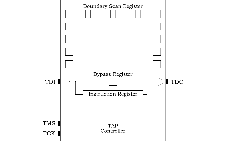
IEEE 1149.1 describes a simple architecture for chips implementing
boundary scan testing. In its minimal configuration, it provides
four external pins, a clock (TCK), data in (TDI), data out
(TDO) and a management signal (TMS). Collectively these pins are
known as the Test Access Port (TAP).
Internally there are two registers in addition to the boundary scan register: the instruction register and the bypass register. Figure 2.6 shows this minimal architecture.
Bits are shifted in on the positive edge of TCK and shifted out on
the negative edge. The TMS signal is used to control the register
into which the bits are shifted (instruction register, bypass
register or boundary scan register). TMS usage is described more
fully below.
The basic cycle of operation is a sequence of
capture a register, shift
in a new value from TDI, while simultaneously shifting out the old
value on TDO, then update the register with the
value shifted in.
The TAP controller can shift values either through the instruction register or through one of the other registers (collectively known as data registers). In the minimal configuration there are only two data registers: the boundary scan register and the bypass register. The bypass register is a convenient mechanism when boundary scan testing is not being used.
The instruction register must be at least 2 bits long. IEEE 1149.1 requires a minimum of 4 instructions:
BYPASSCapture, shift and update data through the bypass entry. This allows the chip to continue its normal operation. IEEE 1149.1 requires this instruction to consist of all 1's.
SAMPLECapture and shift data through the boundary scan register, thus taking a sample of the data entering and leaving the chip via its inputs and outputs. However the update phase does not drive data onto inputs or outputs.
PRELOADShift data through the boundary scan register, thus setting up a value in the scan cells for future use. For this instruction, the capture phase does not get the previous value into the cell and the update phase does not drive data onto inputs or outputs.
In early versions of the standard, this instruction was
combined with SAMPLE.
EXTESTThe chip is placed in extest mode before data is captured, shifted and updated through the boundary scan register.
This is used to test connectivity between multiple chips. In
extest mode the chip does not try to
drive outputs or accept inputs. It is normal to use
PRELOAD to set up the boundary scan
register prior to EXTEST.
Early versions of IEEE 1149.1 required this instruction to consist of all 0's, although this is not the case in more recent versions.
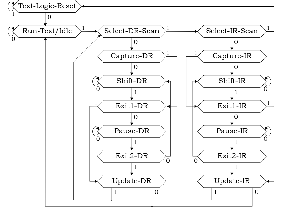
The TCK and TMS signals drive a finite state machine in the TAP
controller. TMS is sampled on the rising edge of TCK and used to
advance the state. The state machine is shown in Figure 2.7.
The actions taken in each state are as follows:
In this state all test-modes (for example extest-mode) are reset, which will disable their operation, allowing the chip to follow its normal operation.
At start-up the external logic will drive TMS high for at
least 5 TCK cycles. This guarantees to reach the
Test-Logic-Reset state and remain there.
This is the resting state during normal operation.
These are the starting states respectively for accessing one of the data registers (the boundary-scan or bypass register in the minimal configuration) or the instruction register.
These capture the current value of one of the data registers or the instruction register respectively into the scan cells.
This is a slight misnomer for the instruction register, since it is usual to capture status information, rather than the actual instruction with Capture-IR.
Shift a bit in from TDI (on the rising edge of TCK) and out
onto TDO (on the falling edge of TCK) from the currently
selected data or instruction register respectively.
These are the exit states for the corresponding shift state. From here the state machine can either enter a pause state or enter the update state.
Pause in shifting data into the data or instruction
register. This allows for example test equipment supplying
TDO to reload buffers etc.
These are the exit states for the corresponding pause state. From here the state machine can either resume shifting or enter the update state.
The value shifted into the scan cells during the previous states is driven into the chip (from inputs) or onto the interconnect (for outputs).
So we have a simple state machine, which allows either data registers or the instruction register to go through its capture-shift-update cycle, with an option to pause during the shifting.
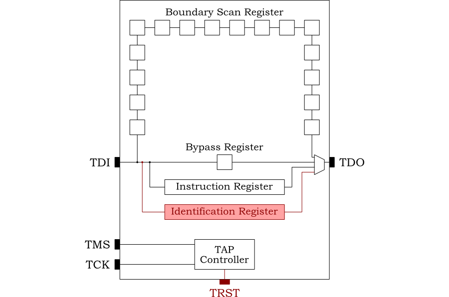
IEEE 1149.1 specifies an optional asynchronous reset pin, TRST,
an optional identification register and a number of optional
instructions that may be included. The extended architecture is
shown in Figure 2.8.
The reset pin, TRST, is active low. If driven low it immediately
takes the state machine to the Test-Logic-Reset state.
![[Note]](../images/note.png) | Note |
|---|---|
If |
The device identification register is a
32-bit data register. It identifies version and part number for
both manufacture and user. It can be read using the optional
ICODE and USERCODE
instructions.
Additional instructions also support INTEST
(like EXTEST, but with on-chip test data),
RUNBIST (to run comprehensive
Built-in Self Test logic),
CLAMP (to clamp outputs to predefined logic
levels) and HIGHZ (to set all outputs to the
disabled (high impedance) state).
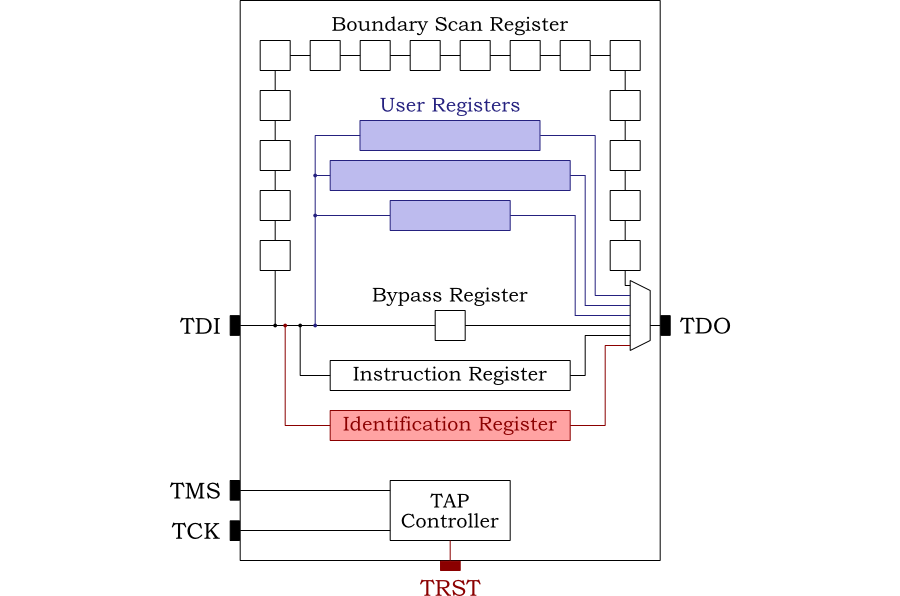
JTAG provides a generic mechanism for accessing registers on chip. The standard allows the architecture to be extended with user registers, accessed using the user's own instructions. Figure 2.9 shows how these registers may be added.
The user will add their own instructions to access these additional registers. This is a common mechanism to interface to debug units on modern system-on-chip (SoC) designs.
| |  | |
| 2.1.1. Boundary Scan |  | 2.2. OSCI SystemC IEEE 1666 |