What is RI5CY?
RI5CY is a 4-stage in-order pipelined RISC-V core written in SystemVerilog. It has become very popular for many applications, including being adopted as the first Core-V core in the OpenHW Group family, as well as being proposed as the reference for EmBench, a benchmark for embedded processors initiated by David Patterson and introduced at the RISC-V Workshop in Zürich ( Slides | Video ).
It has become popular because it provides a good starting point for customisation – it is well-maintained, clear SystemVerilog, and can easily be instantiated using synthesis or simulation tools – for example, it comes with a testbench for a Verilator model, and has both flip-flop and latch register files for efficient instantiation on FPGAs or ASICs. It balances complexity with customisability well.
Why look at RI5CY internals?
Because it is a good starting point for customisation, I am working on two projects involving RI5CY:
- integrating the XCrypto side-channel-resistant cryptographic ISE into the design (more details on this, in a blog post to follow).
- Developing a workshop tutorial in adding new instructions to RI5CY, which will be held as part of the Open Source Hardware Camp, on 31st August and 1st September.
This post is a dive into two aspects of the RI5CY implementation, the decoder and register file – these need to be understood to make modifications that add additional instructions.
The Decoder
Background: Compressed instructions
RI5CY supports the Compressed, “C”, instruction extension. C instructions are 16 bits wide, as opposed to the usual 32 bit RISC-V instructions, and can greatly reduce code size / increase code density. In RISC-V, compressed instructions are aliases for full 32 bit instructions, rather than a separate set of instructions, and there is a one to one mapping between 16-bit compressed instructions and 32 bit instructions. This works because the C instructions are versions of the full-sized instructions which fulfil some of the following conditions (depending on the specific instruction):
- The immediate or address offset is small
- One of the registers is the zero register (x0), the ABI link register (x1), or the ABI stack pointer (x2)
- The destination register and the first source register are identical, or
- the registers used are the 8 most popular ones.
Compressed instructions can be mixed in with standard instructions, so all that is needed to execute these instructions is a module in the fetch stage to expand the instruction from its compressed form to the standard form. The assembler can generate compressed instructions whenever the instruction being assembled fulfils the necessary conditions for emitting a compressed instruction.
16-bit instructions on ARM vs. RISC-V
Having looked at how RISC-V deals with compressed instructions, it is worth having a brief look at how another RISC architecture does this. ARM’s compressed instructions are called Thumb instructions, and they execute in a separate “Thumb mode” – this mode is distinguished from “ARM mode” by setting a bit in the Program Counter. The program switches into and out of Thumb mode by branching to addresses that have the least significant of the address set to 1 or 0 respectively. As a result, it is not possible to intermingle ARM and Thumb instructions, and the assembler must specifically emit either ARM or Thumb code for a sequence of instructions, rather than having a free choice of which instructions to emit.
Thumb instructions don’t have a one to one mapping for all ARM instructions. From the perspective of designing the instruction set, this is a slightly more relaxed constraint than that for the design of RISC-V C instructions. This, coupled with the use of instructions such as load / store multiple in ARM, results in ARM/Thumb code density being slightly better than RISC-V in most cases. For an in-depth comparison of code size on ARM, RISC-V, and ARC (another RISC architecture) see How Compact is Compiled RISC-V Code? ( slides | video ) by Jeremy Bennett at FOSDEM 2019.
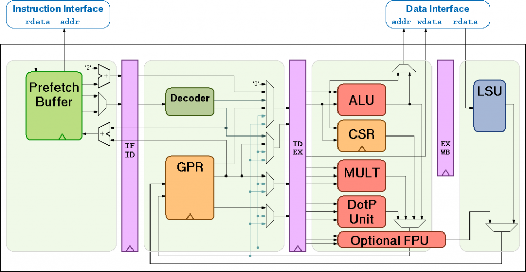
The RI5CY Fetch stage
The process by which the RI5CY core decodes an instruction starts in the instruction fetch stage (riscv_if_stage). Inside the fetch stage, the prefetcher (riscv_prefetch_buffer) handles reading instructions from memory. To accommodate one of the RI5CY extensions (hardware loop instructions) it is capable of detecting compressed instructions in order to adjusting the length it reads when a hardware loop is being executed.
Instructions from the prefetcher are passed to the riscv_compressed_decoder module:
  riscv_compressed_decoder
    #(
      .FPU(FPU)
     )
  compressed_decoder_i
  (
    .instr_i         ( fetch_rdata          ),
    .instr_o         ( instr_decompressed   ),
    .is_compressed_o ( instr_compressed_int ),
    .illegal_instr_o ( illegal_c_insn       )
  );
The compressed decoder in the fetch stage takes in 32 bits read from the instruction prefetch buffer. If these bits hold a compressed instruction, then it outputs the decompressed variant of the instruction, and signals that there is a compressed instruction. Since some instructions that appear to be compressed instructions may also be illegal instructions (the compressed encoding space is not fully dense) it can also signal an illegal compressed instruction. These signals are then passed to the decode stage.
The RI5CY Decoder
RI5CY’s decoder is more complex than the fetch stage, so in this section we will look at an overview of its structure, how it detects instruction classes and decodes immediates and registers on a general level. The purpose of the decoder is to set up signals to control the execution stage based on the current encoded instruction, e.g.:
- Which unit should operate,
- What operations it should perform,
- What operands it should perform them on.
Parameters and some preamble
First the decoder sets up some local parameters which define how to decode some instructions. These define things such as whether the processor has a floating point coprocessor, which affects how the instruction is decoded later on. Next some signals are defined which are processed in the decoder to determine whether it is necessary to perform certain actions later on in the execution stage.
An example of one of these signals is csr_illegal, which is used to determine whether an instruction trying to access the Control and Status Registers (CSRs) is allowed to based on the current privilege level. There is a comparison done in the decoder between the permission required by the instruction being decoded and the current permission level – if the required level is greater than csr_illegal is set to 1, which later on sets illegal_insn_o, an output which signals that a decoded instruction was invalid.
Main decoding switch
Next is the main part of the decoder. This is a large case statement that decides what to do based on which bits are set in the instruction.At the highest level, the switching is based on the opcode of the instruction. The top of the case statement, showing selection of the opcode, and the first instance (for the JAL instruction) is shown below:
    unique case (instr_rdata_i[6:0])

      //////////////////////////////////////
      //      _ _   _ __  __ ____  ____   //
      //     | | | | |  \/  |  _ \/ ___|  //
      //  _  | | | | | |\/| | |_) \___ \  //
      // | |_| | |_| | |  | |  __/ ___) | //
      //  \___/ \___/|_|  |_|_|   |____/  //
      //                                  //
      //////////////////////////////////////

      OPCODE_JAL: begin   // Jump and Link
        jump_target_mux_sel_o = JT_JAL;
        jump_in_id            = BRANCH_JAL;
        // Calculate and store PC+4
        alu_op_a_mux_sel_o  = OP_A_CURRPC;
        alu_op_b_mux_sel_o  = OP_B_IMM;
        imm_b_mux_sel_o     = IMMB_PCINCR;
        alu_operator_o      = ALU_ADD;
        regfile_alu_we      = 1'b1;
        // Calculate jump target (= PC + UJ imm)
      end
The JAL instruction saves the address of the next instruction to be executed in its destination register, and branches to the destination address. It is one of the simpler opcodes to implement – the above implements signals to achieve the following:
- Use the ALU to calculate the return address of the instruction (PC + 4)
- Store the result (in
x1by default, though other registers can be used) - Calculate the address of the target instruction
- Write the target address to the PC so that execution resumes from that new address.
There are many more opcodes, all defined in riscv_defines.sv. Another example is the branch opcode, which can perform several different operations – one for each of its variants:
BEQ(Branch EQual),BNE(Branch Not Equal),BLT(Branch Less Than),BGE(Branch Great than or Equal),BLTU(Branch Less Than Unsigned),BGEU(Branch Greater than or Equal Unsigned).
The following code implements the branch instruction in the decoder:
      OPCODE_BRANCH: begin // Branch
        jump_target_mux_sel_o = JT_COND;
        jump_in_id            = BRANCH_COND;
        alu_op_c_mux_sel_o    = OP_C_JT;
        rega_used_o           = 1'b1;
        regb_used_o           = 1'b1;

        unique case (instr_rdata_i[14:12])
          3'b000: alu_operator_o = ALU_EQ;
          3'b001: alu_operator_o = ALU_NE;
          3'b100: alu_operator_o = ALU_LTS;
          3'b101: alu_operator_o = ALU_GES;
          3'b110: alu_operator_o = ALU_LTU;
          3'b111: alu_operator_o = ALU_GEU;
          3'b010: begin
            alu_operator_o      = ALU_EQ;
            regb_used_o         = 1'b0;
            alu_op_b_mux_sel_o  = OP_B_IMM;
            imm_b_mux_sel_o     = IMMB_BI;
          end
          3'b011: begin
            alu_operator_o      = ALU_NE;
            regb_used_o         = 1'b0;
            alu_op_b_mux_sel_o  = OP_B_IMM;
            imm_b_mux_sel_o     = IMMB_BI;
          end
        endcase
      end
To implement the different kinds of branch, it uses a second switch statement on the 12th through 14th bits of the instruction. These bits define which operator is used in the branch, and sets the alu_operator_o signal appropriately for the ALU to perform the necessary comparison operation.
The Register File
RI5CY supports two register files:
- The latch-based register file
- The flip-flop based register file.
There are two different ones because latches are much cheaper in terms of space on ASICs whereas flip-flops are better for a FPGA based implementation. We will look at the flip-flop based register file, as it is more widely used. It is only around 200 lines long, so we can examine most of the blocks in the file.
Parameters and signals
The first part we examine is the parameters. These define the address width and the data width, and whether there is a floating point unit.
- For both the RV32I and E ISAs, the data width will always be 32.
- The address width changes because in RV32E there are only 16 registers, so only need 4 bits are needed to index them. With RV32I there are 32 general purpose registers, and can be 32 floating point registers, so up to 6 bits are needed to index them.
Following the parameters, the input/output signals for the read and write ports are defined.
Memory
The memory that stores integer and floating point register values is defined as 32 arrays of 32 bits each:
  // integer register file
  logic [NUM_WORDS-1:0][DATA_WIDTH-1:0]     mem;

  // fp register file
  logic [NUM_FP_WORDS-1:0][DATA_WIDTH-1:0]  mem_fp;
Register reads
Next is the read address decoder. This works by using the parameters defined at the top of the register file to correctly index either the floating point registers or the integer registers. The decoder also uses the most significant bit of the address being read from to decode which register file is being used.
  //-------------------------------------
  //-- READ : Read address decoder RAD
  //-------------------------------------
  if (FPU == 1 && Zfinx == 0) begin
     assign rdata_a_o = raddr_a_i[5] ? mem_fp[raddr_a_i[4:0]] : mem[raddr_a_i[4:0]]
     assign rdata_b_o = raddr_b_i[5] ? mem_fp[raddr_b_i[4:0]] : mem[raddr_b_i[4:0]]
     assign rdata_c_o = raddr_c_i[5] ? mem_fp[raddr_c_i[4:0]] : mem[raddr_c_i[4:0]]
  end else begin
     assign rdata_a_o = mem[raddr_a_i[4:0]];
     assign rdata_b_o = mem[raddr_b_i[4:0]];
     assign rdata_c_o = mem[raddr_c_i[4:0]];
  end
Register writes
Then the write address decoder uses a for loop to generate the combinatorial logic for setting the decoded write address signal.
  always_comb
  begin : we_a_decoder
    for (int i = 0; i < NUM_TOT_WORDS; i++) begin
      if (waddr_a == i)
        we_a_dec[i] = we_a_i;
      else
        we_a_dec[i] = 1'b0;
    end
  end
Finally there is the write operation which starts off by tying R0 to zero:
    //-----------------------------
    //-- WRITE : Write operation
    //-----------------------------
    // R0 is nil
    always_ff @(posedge clk or negedge rst_n) begin
      if(~rst_n) begin
        // R0 is nil
        mem[0] <= 32'b0;
      end else begin
        // R0 is nil
        mem[0] <= 32'b0;
      end
    end
Then, some sequential logic and the address decoded earlier are used to assign the data from the write ports into the registers:
    // loop from 1 to NUM_WORDS-1 as R0 is nil
    for (i = 1; i < NUM_WORDS; i++)
    begin : rf_gen

      always_ff @(posedge clk, negedge rst_n)
      begin : register_write_behavioral
        if (rst_n==1'b0) begin
          mem[i] <= 32'b0;
        end else begin
          if(we_b_dec[i] == 1'b1)
            mem[i] <= wdata_b_i;
          else if(we_a_dec[i] == 1'b1)
            mem[i] <= wdata_a_i;
        end
      end

    end

    if (FPU == 1) begin
      // Floating point registers
      for(l = 0; l < NUM_FP_WORDS; l++) begin
        always_ff @(posedge clk, negedge rst_n)
        begin : fp_regs
          if (rst_n==1'b0)
            mem_fp[l] <= '0;
          else if(we_b_dec[l+NUM_WORDS] == 1'b1)
            mem_fp[l] <= wdata_b_i;
          else if(we_a_dec[l+NUM_WORDS] == 1'b1)
            mem_fp[l] <= wdata_a_i;
        end
      end
    end
Further reading / resources
- The RI5CY User Manual: Outlines how to use the RI5CY core as part of a design, and describes the
Xpulpcustom ISA extension that it implements. - The RISC-V Reader: An overview of the RISC-V ISA and the rationale behind many of its design decisions.
- The RISC-V Unprivileged ISA Specification v20190608-Base-Ratified: Defines the RISC-V unprivileged architecture (i.e. not the machine- and supervisor-modes). This includes documentation of all the instructions that would normally be used in typical application executables, including their encodings and semantics.
- The Xcrypto ISA extension: This repository contains links to the Xcrypto ISA extension documentation and reference implementations.
- Attend the Open Source Hardware Camp in Hebden Bridge on 31st August and 1st September 2019, including a talk and workshop on customising the RI5CY core with new instructions.
Next steps
Following this post, I am working on:
- Putting together materials for the Open Source Hardware Camp tutorial – materials will be available online after the event.
- Implementing the Xcrypto extension in RI5CY
- In my next blog post, I will go into Xcrypto and its integration into RI5CY in further detail.
About the Author
Sam Leonard has returned to Embecosm to work on extending RI5CY with Xcrypto instructions over the Summer of 2019, having recently completed A-levels in Maths, Further Maths, Computer Science, and Physics. When Sam joined Embecosm for work experience last summer, he developed a proof-of-concept exploit demonstrating the efficacy of a compiler technique to protect secret data. He will be starting a BSc. (Hons) in Computer Science at the University of Manchester in September.